I’m one of those people who are somehow under-experienced and overqualified at the same time. I’ve done a lot, learned a lot, built a lot — but most of it doesn’t fit neatly into a corporate checkbox. I’ve worked across science, manufacturing, and product development. I’ve led teams, built machines, launched new processes, and solved production issues others gave up on. But because I’ve done things my own way — through startups, side-projects, and hands-on work — I often don’t “look right on paper.” I don’t care much for job titles. I care about doing good engineering: making things that are precise, practical, and actually useful. I thrive when I get to fix messy processes, design tools from scratch, and turn chaotic ideas into clean solutions. If you need someone who can bridge science and production, who understands both the lab bench and the shop floor — that’s where I do my best work.
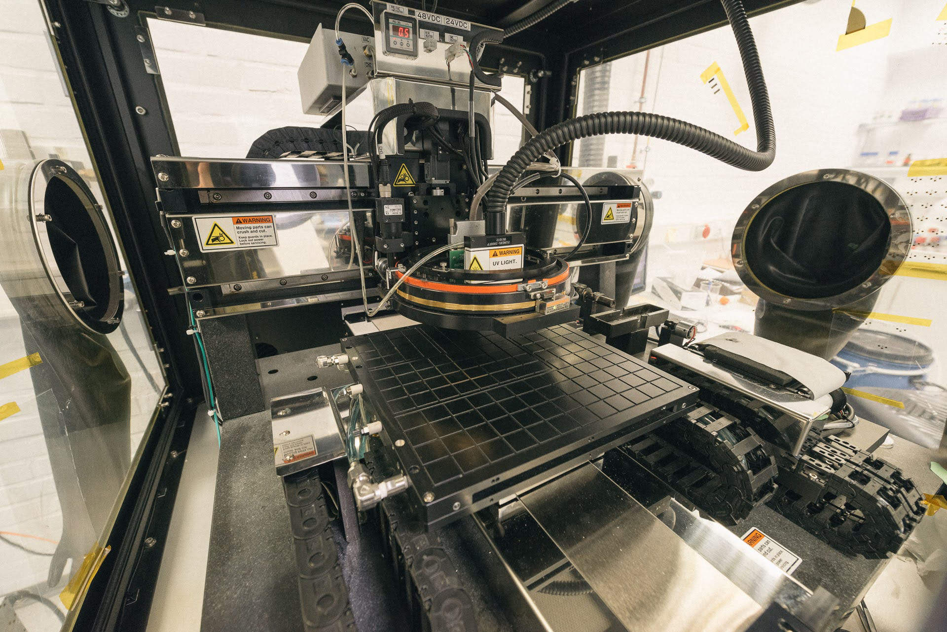
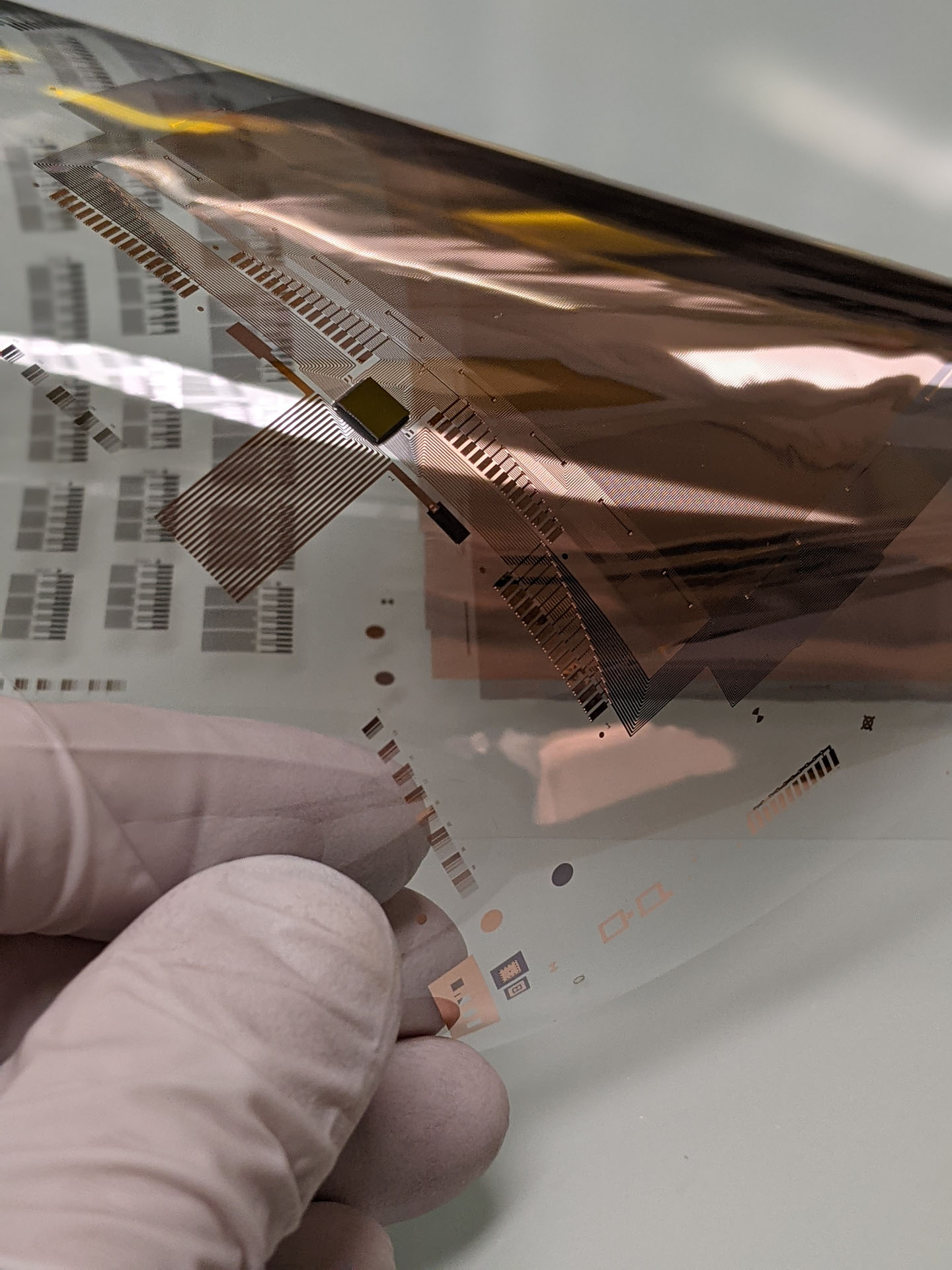
I didn’t get into inkjet printing because it was trendy. I got into it because I needed a way to deposit functional materials with precision — without million-euro equipment. Inkjet gave me freedom: to experiment, to iterate, to hack physical matter at the microscale. Over time, I developed nanoparticle inks, printed optics, anti-counterfeiting structures, and sol-gel systems for photonic coatings — often building the equipment and processes myself. I’ve worked on holograms, biosensors, and functional surfaces, pushing what’s possible with drop-on-demand systems. Inkjet printing isn’t just “printing with liquid.” It’s an entire world of fluid dynamics, materials chemistry, surface science, and frustration. I’ve spent weeks tuning viscosities, nozzle firing sequences, surface energies — just to get a line that dries right and create beutiful new properties.
|
|
|
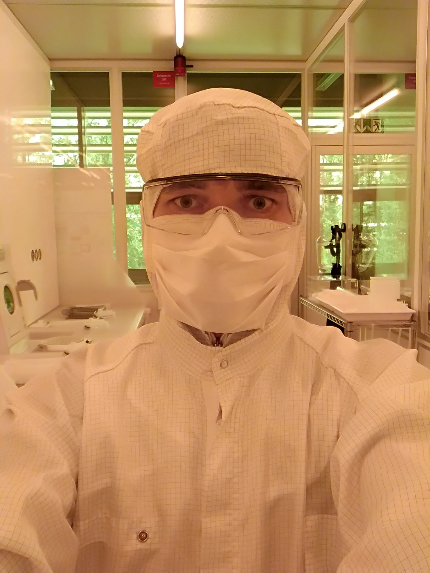
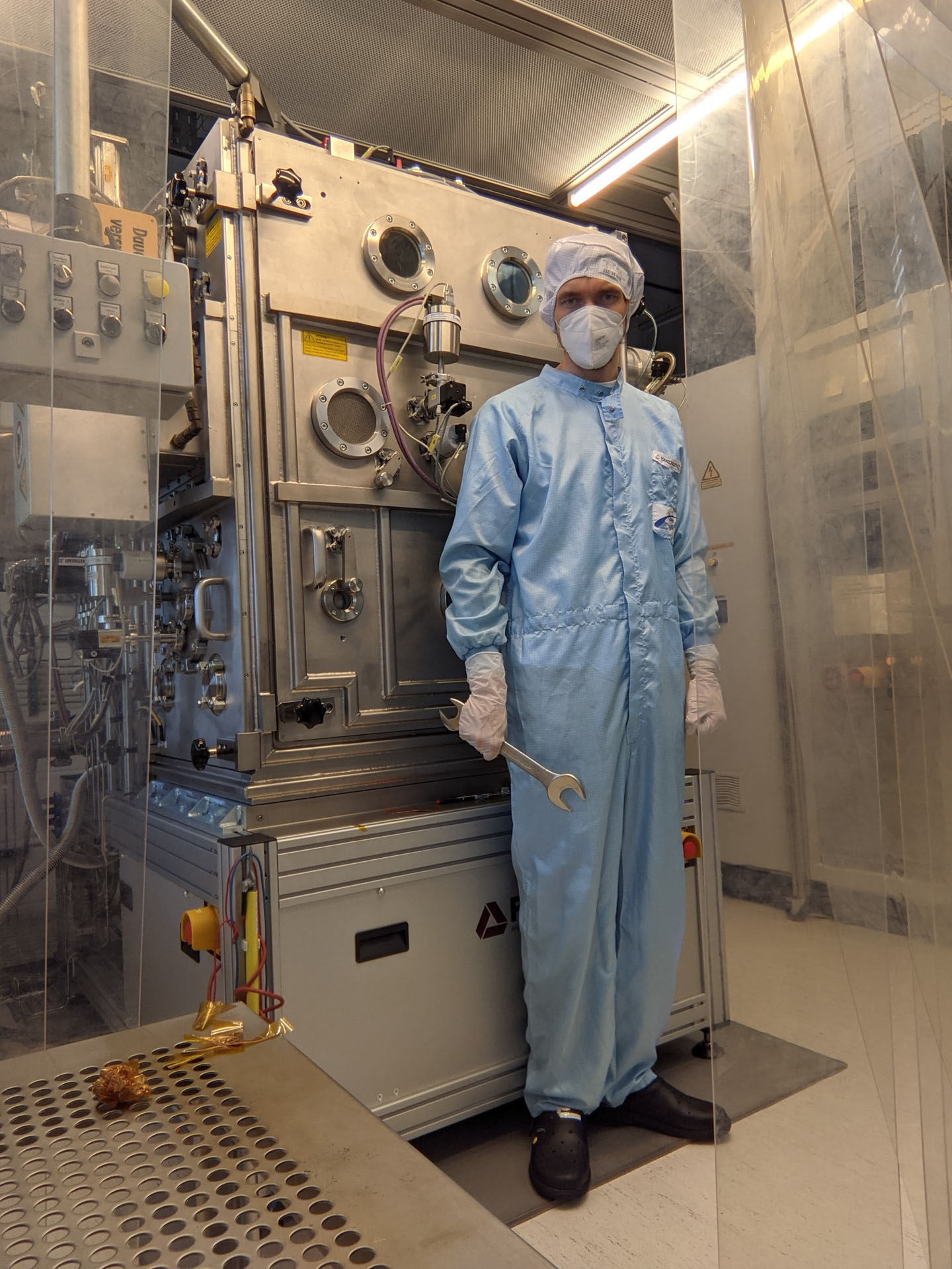
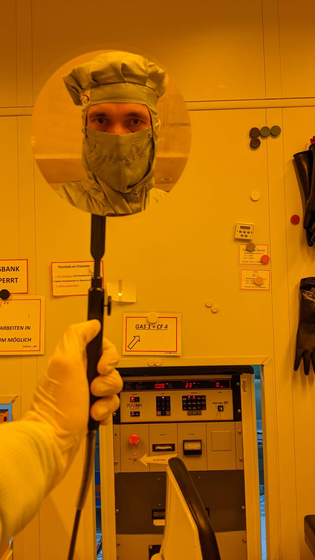
Cleanroom work taught me patience, precision, and respect for the process. I’ve spent years working with thin films and flexible substrates — not in ideal lab conditions, but in real, evolving environments where you have to make things work with what you have. I worked with vacuum deposition systems to coat flexible films, developed roll-to-roll processes for both printing and etching, and got my hands dirty (figuratively — gloves on) with laser ablation, photomask alignment, plasma treatment, and selective masking. Often I had to invent parts of the process on the fly — no textbook, no manual, just understanding the physics and hacking it into shape.
|
|
|
|
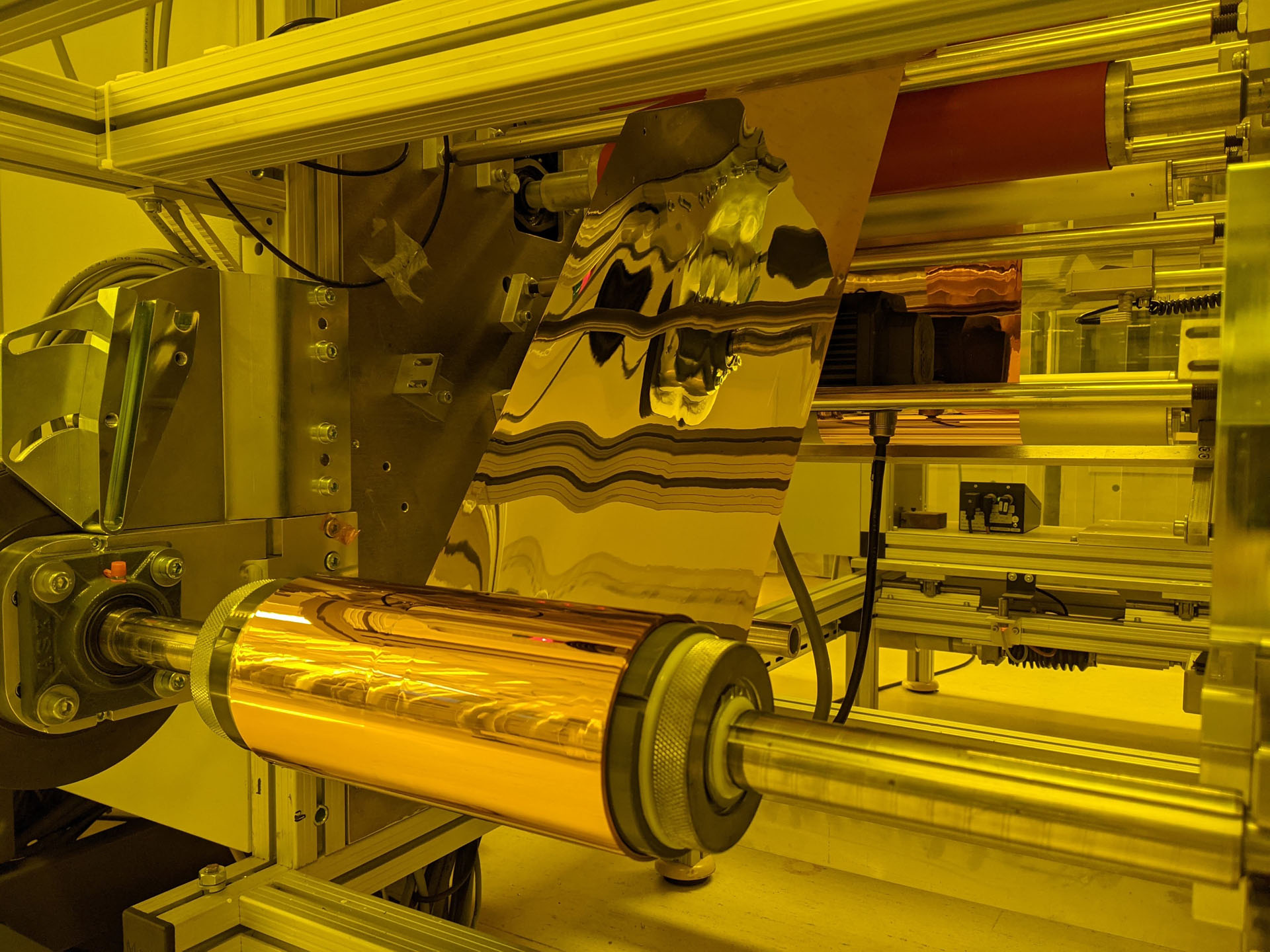
Most of my roll-to-roll work revolved around screen printing and thin-film circuit fabrication — not in some ideal lab, but in the kind of setup where everything had to be hacked, tuned, or rebuilt from scratch to actually work. I worked with polymer substrates like PET and PEN, developed multi-step processes for printing conductive layers, and handled vacuum deposition of metals on flexible films. I also dealt with all the problems nobody talks about — like registration drift, film warping, and ink bleeding when the humidity’s wrong by 5%.
|
|
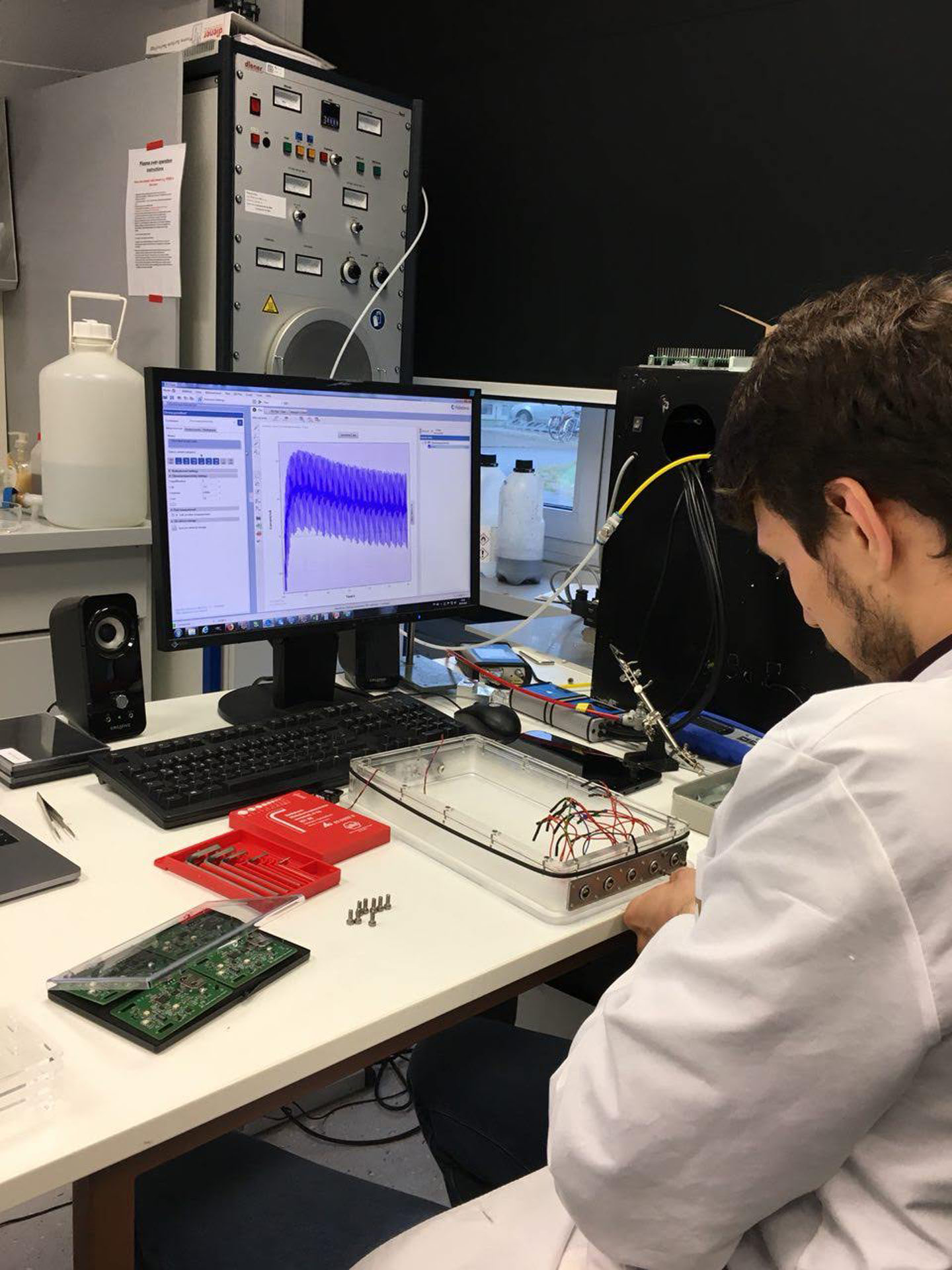
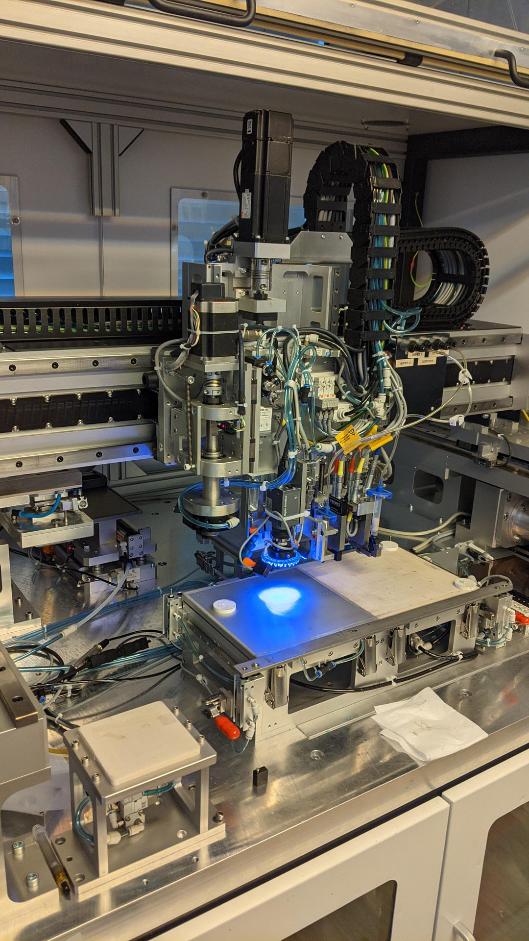
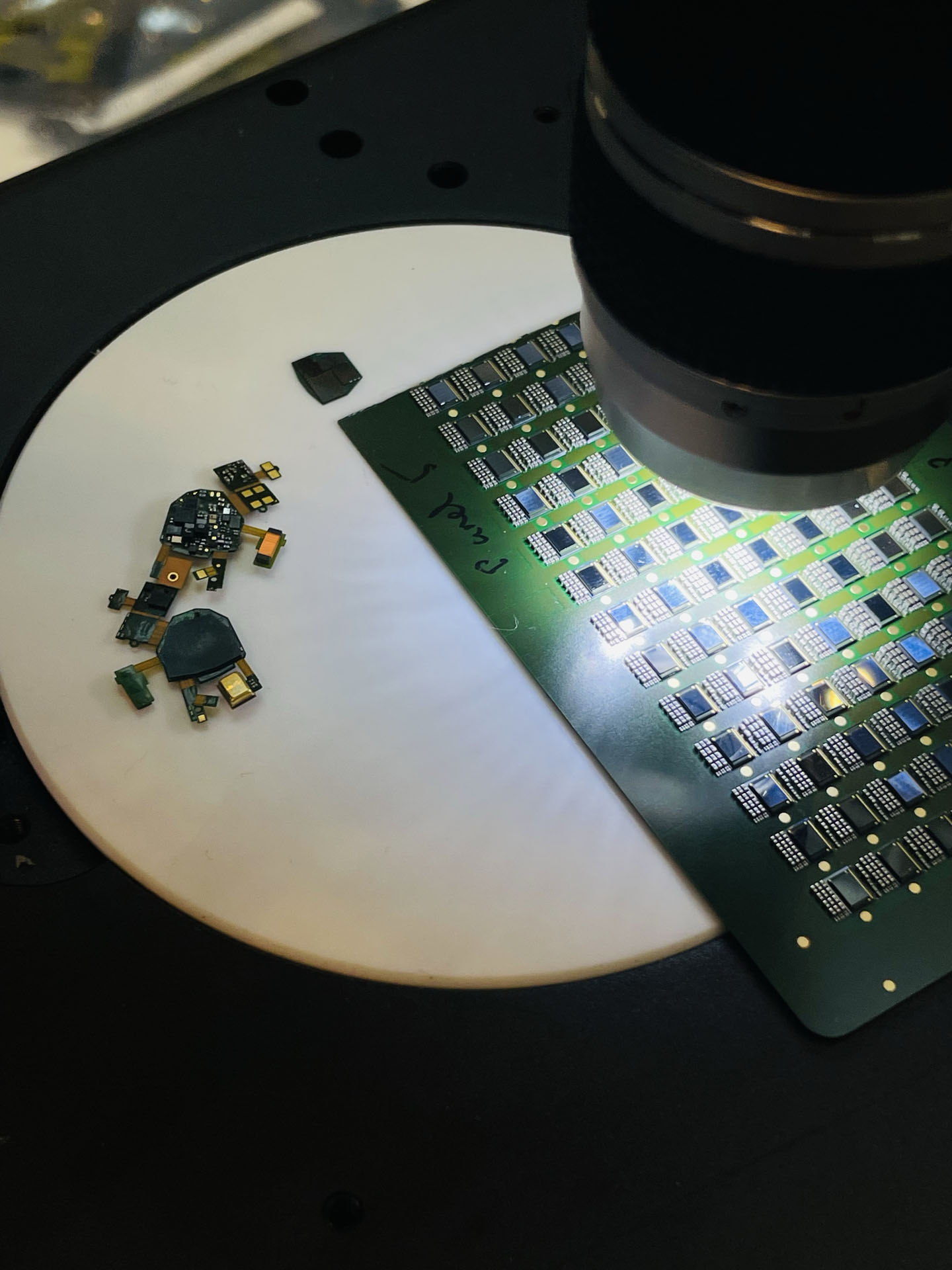
These days, my microelectronics work is centered around packaging and process engineering — the gritty, high-stakes part where devices go from wafer to usable hardware with high-density. I work with hearing aid components and advanced miniaturized assemblies, often dealing with 0201-size passives, 25 μm gold wire bonding, and high-density multi-die setups. Most people think chip packaging is clean and precise — in reality, it's a battlefield of yield loss, thermal mismatch, and mechanical stress and warpage. I spend my days troubleshooting design and assembly problems, optimizing soldering footprints, adjusting parameters on the assembly line, or redesigning the entire process just to make the damn thing work.
Packaging here isn’t just sticking a chip in a box. It’s a complex dance of process preparation, adhesive curing, bonding, encapsulation, and inspection — all under microscope, under specific conditions, and usually under a tight deadline of product releases.
|

|
My role blends hands-on lab work with system-level thinking: How does this tiny interconnect behave during thermal cycling? Why does this board delaminate after two weeks? Can we speed up optical alignment by changing the fixturing? I work with production, R&D, and quality — often acting as the only person who speaks all three dialects fluently.
Most importantly: I don’t just follow the process. I question it, redesign it, and make it robust enough that even the night shift can run it without breaking things. That’s microelectronics to me — not glamorous, but precise, fragile, and incredibly satisfying when you finally get it to work.